We have compiled a list of manufacturers, distributors, product information, reference prices, and rankings for Insulation material punching process.
ipros is IPROS GMS IPROS One of the largest technical database sites in Japan that collects information on.

Insulation material punching process - List of Manufacturers, Suppliers, Companies and Products | IPROS GMS

Insulation material punching process Product List

1~3 item / All 3 items

Displayed results

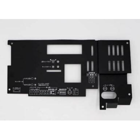
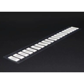
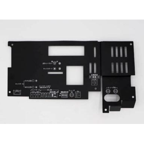
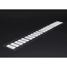
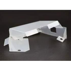
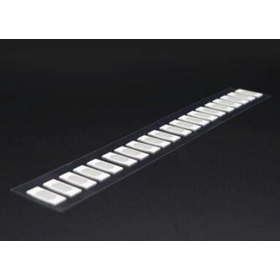
Insulation material punching process for semiconductor manufacturing (PET/PI/PC)

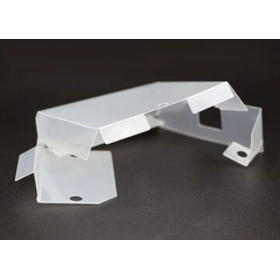
It is also possible to perform punching processing on multilayer laminated materials! Complex bending processing can also be done.

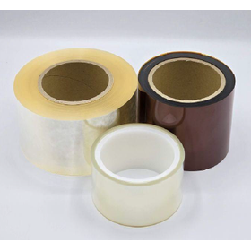
In the semiconductor manufacturing industry, precise component processing in a clean environment is essential to ensure product quality and reliability. In particular, insulating materials for electronic components are a crucial factor that affects product performance, and contamination or dimensional errors can lead to product defects or performance degradation. Our insulating material processing is designed for operations in a clean environment, providing high-quality products through material selection and precision processing techniques tailored to our customers' needs. 【Application Scenarios】 - Punching processing of insulating materials in semiconductor manufacturing processes - Precision component processing in clean rooms - Manufacturing of insulating materials for electronic device substrates 【Benefits of Implementation】 - Reduces the risk of contamination and contributes to improved product quality - Minimizes dimensional errors through precision processing techniques, maximizing product performance - Provides optimal insulating materials through tailored material selection and processing proposals to meet customer needs.

  • 絶縁材加工2.png
  • 絶縁材加工3.png
  • 絶縁材加工4.png
  • Other polymer materials
  • Processing Contract
  • Insulation material punching process

Added to bookmarks

Bookmarks list

Bookmark has been removed

Bookmarks list

You can't add any more bookmarks

By registering as a member, you can increase the number of bookmarks you can save and organize them with labels.

Free membership registration

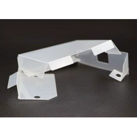
Insulation material punching processing for displays (PET/PI/PC)

Contributing to thin displays! Punching and bending processing of insulating materials.

In the display industry, there is a demand for both miniaturization and the protection and insulation of electronic components. Particularly in thin displays that implement many components in a limited space, the precise processing of insulating materials significantly affects the reliability and safety of the product. Improper use or processing of insulating materials can lead to shorts or failures. Our insulation processing utilizes materials such as PET, PI, and PC to meet the needs for miniaturization while providing high insulation performance. 【Application Scenarios】 - Thin televisions and monitors - Smartphones and tablets - Wearable devices 【Benefits of Implementation】 - Achieving both miniaturization and insulation - Protection of components and improvement of product lifespan - Flexible responses through diverse materials and processing methods

  • 絶縁材加工2.png
  • 絶縁材加工3.png
  • 絶縁材加工4.png
  • Other polymer materials
  • Processing Contract
  • Insulation material punching process

Added to bookmarks

Bookmarks list

Bookmark has been removed

Bookmarks list

You can't add any more bookmarks

By registering as a member, you can increase the number of bookmarks you can save and organize them with labels.

Free membership registration

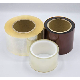
[For Defense] Insulation Material Punching Processing (PET/PI/PC/PP)

It is also possible to punch processed materials with multiple layers! Complex bending processes can also be performed.

In the defense industry, the reliability and durability of electronic devices are extremely important. Products that can withstand use in harsh environments are required, and the selection of insulating materials is a crucial factor that affects their performance. Deterioration of insulating materials can lead to malfunctions or failures of electronic devices, potentially causing serious incidents. Our processing of insulating materials uses materials such as PET, PI, and PC to provide optimal solutions that enhance durability and reliability. 【Application Scenarios】 - Military electronic devices - Aerospace equipment - Communication devices 【Benefits of Implementation】 - Protection of electronic devices in harsh environments - Extension of product lifespan - Assurance of high reliability

  • 絶縁材加工2.png
  • 絶縁材加工3.png
  • 絶縁材加工4.png
  • Other polymer materials
  • Processing Contract
  • Insulation material punching process

Added to bookmarks

Bookmarks list

Bookmark has been removed

Bookmarks list

You can't add any more bookmarks

By registering as a member, you can increase the number of bookmarks you can save and organize them with labels.

Free membership registration